國立台灣大學林清富教授實驗室
研究領域摘要
主題一:有機無機太陽能電池
研究人員:黃敬舜、周貞佑、劉孟岳、蔡國華、王鼎鑫、陳柏諭、林信伯、林宇宏、王膺傑
英文摘要:
Polymer solar cells (PSCs) have attracted much attention due to their great potentials for large-area, light-weight, flexible, and low-cost devices. Recently, bulk-
heterojunction (BHJ) solar cells based on poly(3-hexylthiophene) (P3HT) and (6,6)-phenyl C61 butyric acid methyl ester (PCBM) with power conversion
efficiency (PCE) of 4-5 % have been reported. However, control of the transportation of the charge carriers at interfaces is one of the most challenging issues in
the improvement of PSCs. It has been reported that the insertion of an interlayer between the organic layer and the anode improves the device performance. To
date, poly(3,4-ethylenedioxythiophene):poly(styrenesulfonate) (PEDOT:PSS) and transition metal oxides have been employed for this purpose. However, only
the deposition of PEDOT:PSS layer can be easily processed by solution-based coating techniques. Most transition metal oxides as the anode interlayers are
deposited by the vacuum evaporation, which could detract from the advantage of the ease of PSC fabrication. Using solution-processed transition metal oxide as
the anode interlayer for improving the PSC performance has seldom been reported.
The aim of this work is to realize a low-cost and high-efficiency inverted PSC hybridized with ZnO nanorod arrays by introduction of a solution-processed
vanadium oxide (V2O5) as the anode interlayer. Our investigation shows that the photovoltaic device performance is improved by the introduction of the V2O5
interlayer due to the efficient suppression of the leakage currents at the organic/metal interface. Compared to the conventional BHJ structure (indium tin oxide
(ITO)/PEDOT:PSS/active layer/Al), the use of the inverted structure overcomes some obstacles such as the facile oxidation of Al and the electrical
inhomogeneities of PEDOT:PSS as well as its corrosion to ITO. The inverted PSCs utilize an air-stable high work-function electrode as the back contact to
collect holes and metal-oxide nanostructures at the ITO to collect electrons. Furthermore, it has been reported that the ZnO nanorods have beneficial effects of
collecting and transporting electrons in the inverted PSCs hybridized with the ZnO nanorods. Our works combine these advantages of V2O5 interlayer and ZnO
nanorods, which thereby suppress the leakage currents and improve the collection and transportation of the charge carriers, resulting in enhancements of PCE,
open-circuit voltage (VOC), and fill factor (FF) of the devices. In addition, the V2O5 interlayer can serve as an optical spacer to increase light absorption,
leading to an increased short-circuit density (JSC). Moreover, the V2O5 interlayer and ZnO nanorod arrays both are fabricated from simple solution-based
processes, which are well-suited for use in high-throughput roll-to-roll manufacturing.
Although PEDOT:PSS layer can be solution processed, its hygroscopic nature is likely to form insulating patches due to the water adsorption, thus degrading the
devices. In contrast, V2O5 is relatively insensitive to water and stable in air. The solution-processed V2O5 interlayer can serve as a barrier preventing oxygen or
water from entering and degrading the photoactive layer. In addition, this approach does not need annealing treatment like PEDOT:PSS nor vacuum equipments,
so it is simple, expeditious, and effective. This is very important for commercial realization of low-cost and large-area printed solar cells.
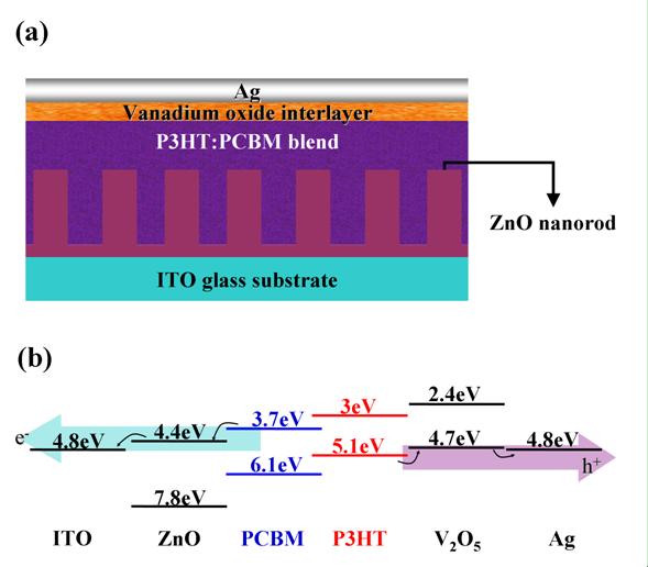
Fig 1. (a) Device structure of the photovoltaic cells. (b) Energy band diagram for the photovoltaic cells in this study.
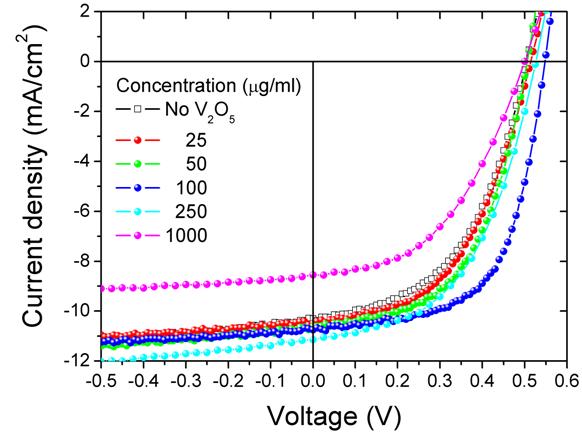
Fig. 2. The J-V curves of the photovoltaic devices with the V2O5 interlayer from various concentrations under 100 mW/cm2 AM 1.5G irradiation.
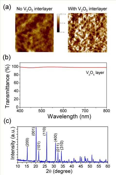
Fig. 3. (a) AFM images of the photoactive layers covered with and without the optimum V2O5 interlayer. AFM image scans are 5×5 μm.
(b) Transmissionspectrum of the V2O5 layer (from the 100 μg/ml V2O5 colloidal solution) on a glass substrate. (c) XRD spectrum of V2O5.
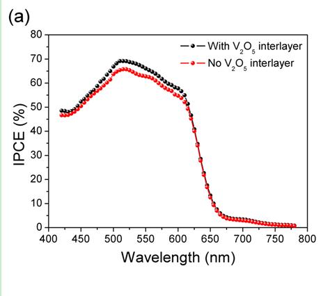
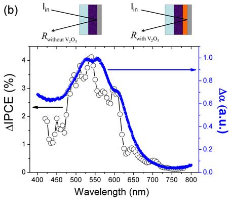
Fig. 4. (a) IPCE spectra for the devices with and without the optimum V2O5 interlayer.
(b) The change in absorption spectrum [Δα(λ)] and the difference in IPCE spectrum [ΔIPCE(λ)] resulting from the insertion of the optimum V2O5
interlayer. The inset is a schematic of the optical beam path in the both samples. The variables are defined in the text.
中文摘要:
與現在矽材料太陽能電池相比,新型有機太陽能電池不僅生?成本低廉、重量輕,而且像塑膠薄膜一樣薄、透明、能夠彎曲,適合製作各種形
狀的太陽能電池,可以廣泛應用在通訊、建築、交通、照明、時尚等領域。新一代有機太陽能電池不僅是對全球氣候變化時期環境保護的貢獻
,而且具有很大的經濟潛力。在元件結構上,一般是使用塊材異質接面(Bulk-heterojunction)結構,以poly(3-hexylthiophene) (P3HT)為電洞傳輸材
料,(6,6)-phenyl C61 butyric acid methyl ester (PCBM)為電子傳輸材料,利用其具大面積激子分離區域的優點,使元件有較佳的效率。然而,載子
在有機/電極介面處的傳輸特性仍有許多改善的空間。文獻指出在有機層與電極中間插入一中介層(interlayer)對於元件效率的改善將有助益。以電
池陽極為例,可以插入poly(3,4-ethylene dioxythiophene):polystyrene sulfonate (PEDOT:PSS)或過渡金屬氧化物作為此用途。然而,只有PEDOT:PSS層
的製作可用簡單的溶液塗佈方式來達成,而作為陽極中介層的過渡金屬氧化物層大多需要真空蒸鍍設備來製作,如熱蒸鍍、濺鍍、電子槍蒸鍍
等。這些真空設備與溶液塗佈方式相較顯得相對昂貴且耗時,亦不利於大面積的應用。有鑒於此,我們的目標是開發出溶液態製備過渡金屬氧
化物作為陽極中介層,並應用於發展低成本且高效率之有機太陽能電池。
我們研究發現導入一層以溶液態製備的五氧化二釩(V2O5)可抑制元件的漏電流進而提升太陽能電池的效率。我們的元件結構與常見的有機太陽
能電池稍不相同。常見的有機太陽能電池結構是氧化銦錫(indium tin oxide, ITO)/PEDOT:PSS/有機主動層/鋁,我們使用的是倒置式結構,此結構以
穩定且功函數高的金屬作為背面電極來收集電洞,同時以ITO為陰極來收集電子,這改善了傳統上鋁電極的易氧化問題與PEDOT:PSS的電荷不均
勻性問題,使電池壽命得以提升。我們結合了V2O5中介層與ZnO奈米柱陣列的優點,除可抑制元件內部漏電流外,也兼顧了電荷的收集與傳輸
,使得有機太陽能電池的效率獲得提升。此外,我們發現V2O5中介層也具有optical spacer的功能,可增加光的吸收,進而增加電池的電流密度。
而且,V2O5中介層與ZnO奈米柱陣列均是以簡單的溶液法製備,非常適合捲軸式的製程(roll-to-roll manufacturing)。
雖然PEDOT:PSS層可以溶液態製備,但它具有吸水性,當吸收了空氣中的水氣後會在PEDOT:PSS層內產生insulating patches,使得元件效率下降。
相反地,V2O5中介層對水氣不敏感,在空氣中相當安定,因此,以溶液態製備的V2O5中介層可作為一屏障,防止水氣與氧氣進入有機層內,使
元件在空氣中較為穩定。此外,由於不需要回火或烘烤,更不需要昂貴的真空蒸鍍設備,我們所使用的方法是相當便利且有效,有助於實現低
成本大面積的有機太陽能電池,對於有機太陽能電池的商業化相當重要。
主題二:晶體型半導體薄膜太陽能電池
研究人員: 趙俊傑
英文摘要:
Because of the significant increase of petroleum and greenhouse effect caused by the carbon dioxide generated from the burning carbon-related fuel, there is an
urgent need of using alternative energy, in particular, the renewable energy sources. Among those renewable energy sources, using solar energy is the most
attractive for its abundant supply form the sun and clean, no pollution characteristics. However, current solar cells are mainly made from bulk Si or bulk III-V
semiconductors. Unfortunately, those types of solar cells need large amount of raw materials, causing the high cost of production. Thus thin-film solar cells are
regarded as good solutions to reduce the material usage.
We propose a novel technique to develop crystalline semiconductor thin-film solar cells. As shown in Fig. 1, the concept is to transfer crystalline Si nano/micro-
structure or III-V compound nano/micro-structure onto alien substrates to fabricate solar cells without lattice-matched concern. This thin-film solar cell with high
crystal quality presents high power conversion efficiency. Besides, the thin-film type offers the advantages of large-area fabrication and the bending flexibility.
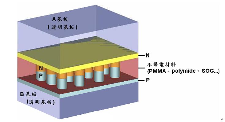
Fig. 1 the conceptual structure of crystalline semiconductor thin-film solar cells
The following is the transfer technique we have developed. InGaP/GaAs double-junction square-based (25μm×25μm) micro-cuboid arrays were released from
GaAs substrate by the epitaxial lift-off process. These InGaP/GaAs micro-cuboid arrays were transplanted to the P3HT film spun on ITO glass substrate
successfully. Besides the significant cost reduction, our method shows the rapid transplantation and the potential for high-efficiency large-area devices
fabrication.
As a result of the ability to tune the band-gap of III-V compound semiconductor materials to match the solar spectrum, solar cells made from these materials
have unsurpassed conversion efficiencies. The most frequently used materials for III–V solar cells such as GaAs and InGaP are direct band gap
semiconductors with high absorption coefficients. A stack with a thickness of only a few micrometers of these materials is required to absorb all light that the
cell can convert into electricity. However, III–V solar cells are usually not referred to as thin-film cells. The reason why III–V cells are not referred to as thin-
film, is that the cell structures are generally deposited on an approximately hundred-μm-thick GaAs or Ge wafer in order to obtain single crystal solar cell
structures.
However, after the deposition of the solar cell film, the substrate is of no further use for its performance. The reduction of the costs of III–V semiconductor
materials and an increase of the power to weight ratio is highly desired. The most successful method to achieve these goals is epitaxial lift-off (ELO). This
method uses a very thin (5-50nm) sacrificial AlxGa1-xAs (x>0.6) release layer which is grown between the device and the GaAs substrate. The thin film device
is released from its host substrate by selective etching of the AlxGa1-xAs release layer with aqueous HF solution, together with the compressive strain induced
by a wax layer. Owing to the large selectivity (>106) of the HF solution for etching of AlGaAs over GaAs, the original substrate is not affected and can be
reused.
A high lateral etch rate is considered essential for industrial applications for ELO technique. Therefore, recently lateral etch rate as obtained by different
approaches of the ELO method has been elaborated in literature, including preparing the samples with wax and submerging them in the HF solution until the
thin films were found floating in the solution after several hours or up to several days, the weight-induced ELO process (WI-ELO), and ELO with a stabilized
radius of curvature by guiding the temporary flexible carrier over a cylinder surface. A disadvantage of the weight-induced ELO process is that the flexible
carrier easily bends too much. This will results in cracking of the epitaxial layer structure. For this reason, the ELO process with a stabilized radius of curvature
by guiding the temporary flexible carrier over a cylinder surface was developed. For the above-mentioned approaches, the larger area of the lifted off epi-film,
the longer time of the ELO etching process and the greater risk of microscopic cleavage cracks. In order to shorten the ELO etching time and prevent the
microscopic cleavage cracks, we develop a unique transplantation method.
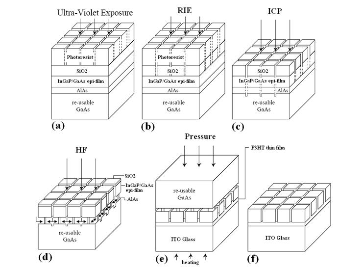
Fig. 2 Sequence of our experimental procedures
Fig. 2 shows the sequence of our experimental procedures. Before growing the InGaP/GaAs double-junction photovoltaic epi-film on the thick GaAs mother
substrate, thin sacrificial AlAs release layer were grown. After the epi-film growth, thick silicon dioxide (SiO2) layer was grown by PECVD. Afterward photo
resist was spun on SiO2 layer and proceed with UV photolithography as shown in Fig. 2(a). The size of each small cubic in the periodic patterns is
25μm×25μm. After photolithography, the patterns were transferred into the SiO2 layer coated on double-junction device by reactive ion etching (RIE) as
shown in Fig. 2(b) and then the photoresist was removed. The etching time was optimized to ensure a reliable pattern transfer, and at the same time to cause the
minimum damage to the surface of double-junction device. After the RIE etching, the periodic square-based (25μm×25μm) patterns were precisely transferred
to the SiO2 mask template as shown in Fig. 3, with a slight increase of the linewidth less than 5%.
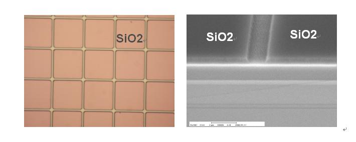
Fig. 3 transfer the periodic cubic patterns into SiO2 layer coated on InGaP/GaAs epi-film
The following procedure is opening a channel down to the sacrificial AlAs release layer by inductive coupled plasma (ICP) etching system as shown in Fig. 4(a)
The ICP etch time was also optimized to ensure the minimum damage to the surface of double-junction device beneath SiO2 mask. After the ICP etching,
the periodic square-based micro-cuboid arrays were accomplished as shown in Fig. 4(b).
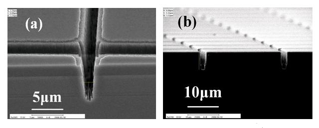
Fig. 4 InGaP/GaAs square-based micro-cuboid arrays. (a) Slots etched by ICP process, (b) Square-based micro-cuboid arrays
Then the sample was submerged in the aqueous HF solution to etch the sacrificial AlAs layer and the remaining SiO2 mask template after ICP etching as shown
in Fig. 2(d). The ELO submerged time must be shorter than the etch time required to completely release the epi-film from the GaAs substrate. After the rapid wet
etching of AlAs layer, there were very tiny AlAs which can remain beneath each cuboid. This tiny AlAs not only fixed each cuboid on GaAs substrate but also
can be snapped easily, as shown in Fig. 5.
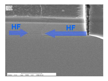
Fig. 5 After ELO, there were very tiny AlAs which can remain beneath each InGaP/GaAs cuboid
The square-based micro-cuboid arrays fabricated above were then transferred to a foreign receiver substrate. The transfer procedure is illustrated in Fig. 2(e).
The receiver substrate was first coated with P3HT [poly (3-hexylthiophene)]. Next, the P3HT was heated. The GaAs wafer with the square-based micro-cuboid
arrays was then pressed against the ITO glass and held there. In the meantime, the micro-cuboid arrays were stuck on the P3HT thin film. Then, the whole setup
was cooled down to room temperature. Various pressures were experimented. Finally, the GaAs host substrate was detached from the ITO glass. After the above
steps, the micro-cuboid arrays were transferred onto the ITO glass as shown in Fig. 6.
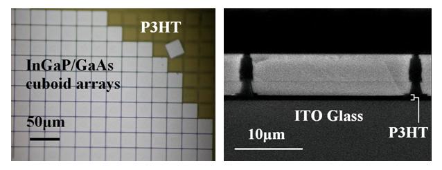
Fig. 6 the images after transferring InGaP/GaAs square-based micro-cuboid arrays on to ITO glass
(Left: top-view, right: cross-section)
We have successfully transferred InGaP/GaAs double-junction square-based (25μm×25μm) micro-cuboid photovoltaic arrays onto the P3HT film spun on
ITO glass substrate using the epitaxial lift-off (ELO) technique. Comparing with the conventional ELO method, including WI-ELO and ELO with a stabilized
radius of curvature, our new method shortens the lifted-off time greatly. Besides, for the above-mentioned approaches, when the area of the lifted off epi-film
becomes larger or the application of the device becomes more bending, the microscopic cleavage cracks may occur. This will limit its application and
performance. However, our new method shows the rapid transplantation and the potential for large-area devices fabrication simultaneously without the cracking
concern. It is expected that a large variety of substrates and much larger area of III-V thin film photovoltaic devices can be used for versatile applications in the
future.
中文摘要:
由於石油價格高漲及石化原料燃燒造成的溫室效應,替代性能源有急迫性的需要,其中太陽能發電是最受矚目的替代性能源。但由於目前太陽
能電池使用矽塊材及III-V族半導體,耗費材料太多,使得成本極高,因此薄膜型太陽能電池被認為是未來的解決方案。
此計畫提出一種創新概念,將發展一套轉移技術用以開發晶體型態的薄膜太陽能元件,如圖一所示,運用的材料包含了目前最常見的矽材料及
高效率光電特性的III-V族材料,主要優勢為克服了基板晶格常數配合的問題,以轉移方式將晶體型態薄膜轉移至各類合適的異質基板上製成太
陽能元件。此型薄膜太陽能電池由結晶良好的晶片蝕刻而得,使得元件保持了原有的良好晶體半導體特性,轉移技術更節省大量的材料成本並
提供了大面積及可撓之前瞻性。
圖一 晶體型半導體薄膜太陽能元件之構想結構
目前我們所發展出來的轉移技術詳述於下,先利用ELO (epitaxial lift-off)技術將InGaP/GaAs雙接面正方形(25μm×25μm)微米柱陣列從GaAs成長基
板上脫離,而後成功轉移至懸塗於ITO透明導電玻璃的P3HT[poly (3-hexylthiophene)]有機薄膜上。此轉移技術除了節省了大量昂貴的基板材料成
本,更具加速製程速度、大面積製作超高效率元件之潛力。
III-V族化合物材料提供了大範圍能階設計的誘人選擇,藉由選擇最佳能隙的半導體材料,以對應於每一個光頻譜範圍,使整體太陽光頻譜得到
最佳使用,最常用來製作III-V族太陽能電池的材料包含了像GaAs、InGaP等具高吸收係數的直接能隙材料。使用串聯堆疊結構,調變接面之能隙
使元件具有更廣大的吸收波長範圍,堆疊結構只需數微米就足以吸收大部分的太陽光頻譜並轉換成電能。然而,III-V族太陽能電池由於磊晶時
晶格常數上的匹配需要,往往須成長於厚度約為幾百微米的GaAs或Ge基板上,因此很少被視為薄膜太陽能電池。
然而,在成長完太陽能電池之串聯堆疊結構薄膜後,成長基板對於太陽能電池效率的表現上並沒有其他功能。因此,移除基板以節省基板材料
成本、同時增加功率對重量比有其需要,其中最成功的技術為ELO (epitaxial lift-off)技術。此技術首先於III-V族多接面磊晶層元件與磊晶成長的基
板間成長一層相當薄(5-50nm)的AlxGa1-xAs (x>0.6)犧牲層(sacrificial layer),蝕刻液為氫氟酸水溶液,主要原理為氫氟酸水溶液對於AlGaAs與
GaAs兩種材料蝕刻情形有相當大的選擇比(>106),藉由選擇性濕蝕刻的方式使III-V族多接面磊晶層元件脫離原本的砷化鎵成長基板,同時,砷化
鎵成長基板將不受影響而仍可重複使用。
側向蝕刻速率在ELO技術的應用上是非常重要的,目前已經有許多ELO技術被發展出來,而其對應的側向蝕刻也同時被報導,包含了:傳統作法
以蠟固定住元件結構再浸泡於氫氟酸水溶液中等待蝕刻完畢而浮起,其過程相當耗時,蝕刻時間往往長達數小時至數天,而後更發展出藉由重
物懸吊式ELO作法(WI-ELO;weight-induced ELO process)及滾輪式ELO作法(ELO with a stabilized radius of curvature)以加速其ELO製程時間,由於懸
吊式ELO容易使元件薄膜過度彎曲而造成微觀的裂縫瑕疵,進而影響到元件品質,因此發展出滾輪式ELO以固定元件薄膜的曲率。然而,對於以
上的ELO作法,由於為單方向蝕刻,導致大面積元件的移除相當耗時,同時在處理大面積轉移時,元件很容易發生微觀的裂縫瑕疵,進而影響
到元件品質。為了加速ELO蝕刻過程並排除微觀裂縫瑕疵的產生機會,我們發展了一種全新的轉移作法。
圖二 構想元件實行流程示意圖
其做法將詳述於下(見圖二): 首先在InGaP/GaAs雙接面磊晶層之太陽能薄膜元件及砷化鎵成長基板間成長一層AlAs犧牲層,以作為ELO (epitaxial
lift-off)之選擇性蝕刻使用。之後在薄膜元件上以PECVD成長一層SiO2層,再以微影技術將圖案化的光阻做為遮罩,如圖二(a)所示,其形狀為正
方形陣列遮罩,正方形之尺寸約為25μm×25μm,接著將此正方形陣列圖案利用RIE乾蝕刻機台轉印至SiO2層,如圖二(b)所示,最後將光阻移除
。對於RIE步驟而言,其蝕刻時間必須精確控制,使得正方形陣列圖案能準確的轉印至SiO2層,同時能不影響到薄膜元件表面。對於此步驟的結
果,如圖三所示,正方形陣列圖案已能準確的轉印至SiO2層,同時正方形間之間距線寬約略增加在5%以下。
圖三 利用RIE乾蝕刻機台將正方形陣列圖案轉印至InGaP/GaAs磊晶層上的SiO2層
接下來的步驟為使用ICP乾蝕刻機台蝕刻InGaP/GaAs雙接面磊晶層,以製作出溝槽深度至AlAs犧牲層的溝槽,如圖四(a)所示,其蝕刻時間也是必
須精確控制,使其不影響到薄膜元件表面,此時,InGaP/GaAs雙接面磊晶層將成為正方面體陣列,如圖四(b)所示。
圖四 InGaP/GaAs正方面體微米陣列 (a) 以ICP乾蝕刻機台製作出溝槽 (b) 正方面體微米陣列
之後進行ELO蝕刻步驟,將磊晶層基板浸泡於氫氟酸水溶液中,如圖二(d)所示,蝕刻時間應略短於AlAs犧牲層完全蝕刻殆盡之前,使得每個正
方面體下方剩下一根相當細小的AlAs柱狀,讓每個正方面體還能固定於基板之上,同時此細小的AlAs柱也很容易將其折斷,如圖五所示。
圖五 經過ELO後,InGaP/GaAs正方面體下方剩下部份的AlAs柱狀
接著,將正方面體微米陣列轉移至異質接載基板上,如圖二(e)所示。此處所使用的異質接載基板為ITO透明導電玻璃,首先在ITO玻璃上懸塗上
P3HT有機薄膜,而後將具正方面體微米陣列之磊晶基板倒置並熱壓於上,待冷卻固化至室溫,此時正方面體微米陣列已黏至該ITO玻璃上。最
後,將原GaAs成長基板移除,成功地將正方面體微米陣列轉移至ITO玻璃上,如圖六所示。
圖六 將InGaP/GaAs正方面體微米陣列轉移至ITO玻璃上之P3HT有機薄膜 (左:俯視圖;右:側面圖)
我們已經成功利用ELO技術轉移InGaP/GaAs正方面體(25μm×25μm)微米陣列轉移至ITO玻璃上之P3HT有機薄膜。相較於其他ELO轉移技術的最
大優點在於,由於ELO技術側向蝕刻速率並不高,若採取一般ELO作法由單方向開始蝕刻,過程過長,導致大面積元件的轉移相當耗時,蝕刻時
間往往長達數小時至數天,蝕刻速率較快的重物懸吊式ELO作法或是滾輪式ELO作法在處理大面積轉移時,元件很容易發生微觀的裂縫瑕疵,進
而影響到元件品質,同時上述兩種ELO作法仍為單方向蝕刻,所以過程仍相當耗時。我們的作法除了ELO蝕刻過程相當迅速,而且排除了微觀裂
縫瑕疵的產生機會,對於在III-V族薄膜型太陽能電池的應用上,以期有大面積製作、同時壓低成本、轉移於適合基板(甚至提供可撓之可能性)、
加速製程速度等應用潛力。
主題三: 矽奈米線太陽能電池應用
研究人員: 許書嘉
英文摘要:
Si nanowires (NWs) attract significant attention because of their potential applications such as vertically integrated NW field effect transistors, bio-chemical
sensors, photovoltaic, thermoelectric devices, lithium battery anodes and so on. Si NWs can be fabricated using chemical vapor deposition, laser ablation,
thermal evaporation, and solution methods. For certain applications, Si NWs are preferred to form on the substrate different from Si. For example, cost and
flexibility may be concerned for solar cells, so metal films, glass, or plastics are preferred. Biocompatibility, light weight, and transparency are important factors
for bio-chemical sensing, so glass or plastics are better than Si. The formation of Si NWs on alien substrates has been achieved using methods such as chemical
vapor deposition. Si NWs have been grown on stainless steel film, but the growth and process temperature is above 650 oC, which is not suitable for plastics or
glass substrate.
Transfer of Si NWs from Si substrate to alien substrates has been proposed and demonstrated for thermoelectric and photovoltaic applications. Even hundreds of
pre-aligned silicon NWs onto plastic has also been achieved. However, those transferred Si NWs are horizontally aligned, limiting the NW density. In addition,
they use the expensive Si-on-insulator (SOI) wafer to start with. Thus the cost is actually large although the devices are fabricated on the cheap plastic. Here we
demonstrate the massive transfer of over millions of Si NWs fabricated from the usual Si wafer onto glass with the density of about 3 - 5 x 10⁷ Si NWs/mm2.
The transferred Si NWs have nearly identical orientation and are vertically aligned on the glass substrate. The X-ray diffraction investigation reveals that the
transferred NWs exhibit almost the same crystal property as the bulk Si. Their characteristics are investigated. The absorption characteristics of the transferred Si
NWs are significantly modified over the spectral range of 400 - 1100 nm. More than 30-fold enhancement of absorption coefficient was found in the near
infrared (IR) range.
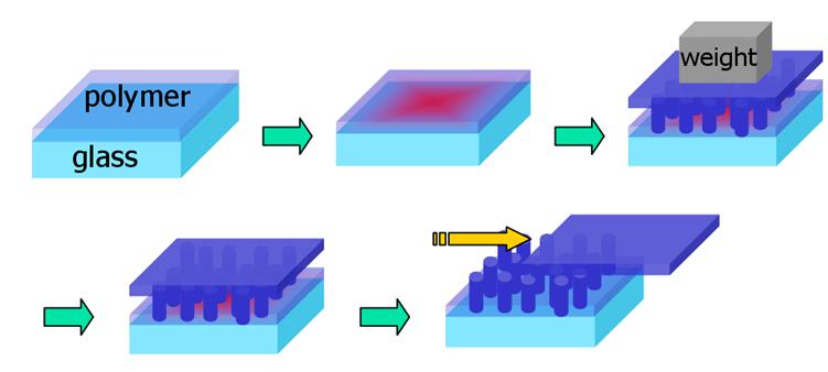
Figure 1 Illustration of massively transferring vertically-aligned Si NWs.
(a) The receiver substrate spin-coated with polymer thin film is heated.
(b) The Si NWs are pressed against the glass substrate.
(c) The whole setup is cooled down until the temperature dropped below the glass transition temperature of polymer.
(d) To remove the original Si substrate.
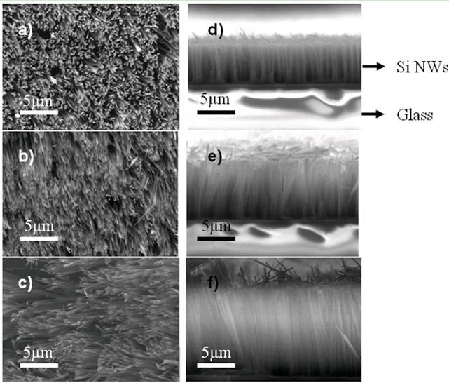
Figure 2 SEM images of transferred Si NWs on glass substrates at the impressing pressure about 55 kg/cm2.
(a)-(c) The top-view SEM images of transferred Si NWs.
(d)-(f) The side-view SEM image of transferred Si NWs on glass substrates.
The lengths of transferred Si NWs are 5.07μm, 6.98μm, and 10.84 μm, respectively.
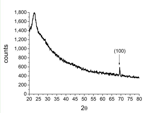
Figure 3 X-ray diffraction spectrum. A sharp peak corresponding to silicon (100) is observed at 69°,
suggesting that transferred Si NWs exhibit total (100) preferential orientation. A broad featureless peak,
centered at about 22°, is assigned to the amorphous silica of the receiver substrate.
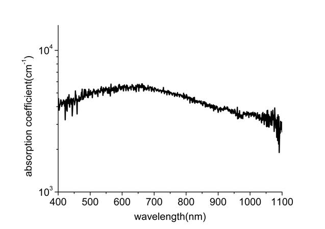
Figure 4 The estimated absorption coefficient of transferred Si NWs.
The absorption coefficient is about 3×103 cm-1 at the wavelength of 1100 nm and increases to a maximum of 5.5×103 cm-1 at 650 nm.
中文摘要:
矽奈米線吸引很多的注意,這是由於他很有潛力應用於場效電晶體、生化感測器、熱電元件等等。矽奈米線的製作可以使用化學氣相沈積法、
雷射法、熱蒸鍍法、和溶液法。在一些應用當中,矽奈米線需要製作於其他基板上,例如在可撓基板上的應用,玻璃或塑膠基板,然而以目前
的方法要將矽奈米線製作於其他基板上,遇到很大的障礙,因為目前的製程環境需要高溫650度以上,玻璃和塑膠基板都無法承受這樣的高溫環
境。
轉移矽奈米線於異質基板上已經有應用於熱電元件與太陽能元件的應用,數百根的奈米線可以被轉移,然而這些奈米線是平行於基板方向,而
限制奈米線的密度,且這些奈米線必須先製作於昂貴的SOI基板上才易於轉移,這使得成本大大地提昇。這裡我們展示可以大量轉移直立矽奈米
線於異質基板上,奈米線的密度達到3 - 5 x 10⁷ Si NWs/mm2。轉移的矽奈米線具有相同的晶格方向性,且於直立排列於基板上。我們研究轉移奈
米線的光學特性,發現轉移於玻璃基板上的矽奈米線的吸收係數產生很大的變化,在紅外光區域的吸收係數增加超過30倍,這項研究成果的發
現,將使矽奈米線在未來很有潛力應用於太陽能電池,增加紅外光區域的吸收。
主題四: 氧化鋅奈米結構及其應用
研究人員: 黃敬舜、李俊育、蘇文彥、周貞佑
英文摘要:
One-dimensional (1D) nanowires have been extensively studied in recent years. Among these materials, zinc oxide (ZnO) nanowires have attracted great interest
for promising applications in optoelectronics devices such as room temperature lasers, light emitting diodes, ultraviolet (UV) detectors, field emission displays,
photonic crystals, and solar cells. ZnO is a wide band gap (3.37 eV) semiconductor with a large exciton binding energy (60meV), exhibiting near-UV light
emission, transparent conductivity, and piezoelectricity. Several methods have been demonstrated to fabricate 1D ZnO nanostructures, such as vapor-liquid-
solid epitaxy (VLSE), chemical vapor deposition (CVD), and pulse laser deposition (PLD), but these gas phase techniques still have some limitations for
substrate size and the need for high temperature operation (above 800 ℃ for VLSE and 500 ℃ for CVD method). Recently, growth of ZnO nanowires and
microrods in aqueous solutions at low temperature was reported by using the hydrothermal process. Hydrothermal process has shown the possibility for
applications in light emitting diodes and solar cells with their growth temperature below 100 ℃ and easy scale-up. This aqueous-based technique has also been
used successfully to demonstrate the fabrication of large arrays of vertical ZnO nanowires on glass, 4-in. diameter Si wafers, and plastic substrates. This
stimulated the study of using ZnO nanowire arrays on plastic substrates for application in flexible electronic devices. However, these device applications might
be reinforced if the position, orientation, and shape of nanostructures can be controlled to a high degree of precision.
This work provides a systematic study of feature-controlled ZnO nanowire arrays via hydrothermal method. Our investigation demonstrates that the sol-gel thin-
film pretreatment conditions have strong influences on the features of the ZnO nanowire arrays grown thereon. The annealing temperature of the ZnO sol-gel
thin film can affect the microstructure of the ZnO grains and then the growth of the ZnO nanowire arrays. As the annealing temperature increases from 130 to
900 ℃, the grain size of the thin films increases, and the diameter of thereon ZnO nanowire arrays increases from 60 to 260 nm. The thin films influence the
nucleation of the ZnO and subsequently affect the diameter and orientation of the thereon nanowire arrays. At the temperature of 130 ℃, the ZnO nanowire
arrays align very vertically with growth along the c-axis direction. The PL measurements show a strong UV emission at 385nm, indicating that the low-
temperature growth results in low levels of oxygen vacancies in the nanowires. This work provides all solution-based processing routes to fabrication of low-
cost highly oriented ZnO nanowire arrays at low temperature. These vertical nanowire arrays are highly suitable for use in ordered nanowire-polymer devices,
such as solar cells and light emitting diodes.
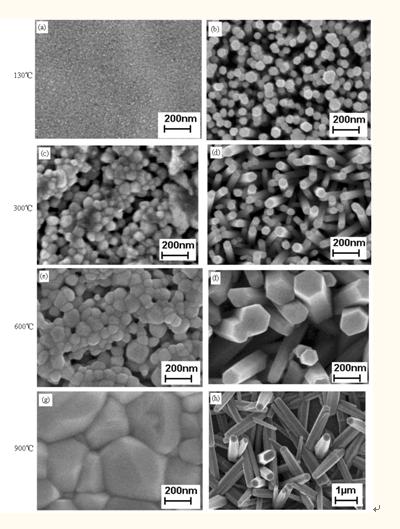
Figure 1 SEM images of ZnO sol-gel thin films with annealing at (a)130℃, (c)300℃, (e)600℃, and (g)900℃. (b), (d), (f), and (h) show the ZnO nanowire
arrays were grown at a fixed temperature (90 ℃), while the thin films were annealed at 130, 300, 600, 900 ℃, respectively.
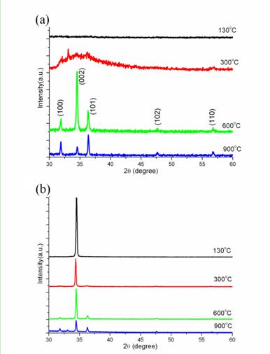
Figure 2 XRD spectra of (a) ZnO seed layers annealed from 130 to 900℃, and (b) thereon ZnO nanowire arrays.
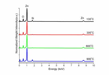
Figure 3 EDS spectra of ZnO nanowire arrays with ZnO seed layers annealed from 130 to 900℃.
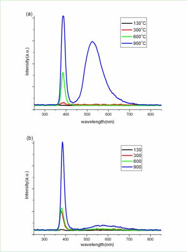
Figure 4 Room temperature PL spectra of (a)ZnO seed layers and (b)thereon ZnO nanowire arrays with annealing temperature of ZnO seed layers from 130 to 900℃ for 1 hour in air (excitation wavelength: 266nm)
中文摘要:
氧化鋅奈米線近年來被廣泛應用於光電元件中,如紫外光雷射、紫外光 LED、紫外光偵測器、氣體感測器、場發射顯示器以及太陽能電池等。
水熱法(Hydrothermal method)是眾多製備氧化鋅奈米線方法中最便宜且可大量製造的方法,然而如何控制氧化鋅奈米線的生長卻是一項重要的課
題。我們利用這個方法可成功製作出方向性一致且單晶的氧化鋅奈米線,並使用場發射顯微鏡(FESEM)、能量散佈光譜(EDS)、X 光繞射(XRD)與
光激發光光譜(PL)來分析氧化鋅奈米線的表面形貌、材料以及光學特性。我們發現氧化晶種層的特性在奈米線的成長過程中扮演相當重要的角色
,經由晶種層的前置處理我們可以改變氧化鋅晶粒的微結構進而有效地控制氧化鋅奈米線的粗細與方向性,此結果對光電元件與奈米元件的應
用將有相當大的助益。
主題五: 光發射光電元件
研究人員: 趙家忻
英文摘要:
In 1879, Thomas Edison invented the light bulb that utilized black-body radiation for illumination. 1 This invention is still in common use today. However the
illumination efficiency remains low because the visible spectrum (400nm-700nm) of black-body radiation occupies only 5% of the total radiation energy even at
the high temperature of 2200 oC. Increasing illumination efficiency is very attractive for the concern of energy consumption. Unfortunately, black-body
radiation is deemed to be of a nature that is difficult to change. Recent advance in research on photonics opens up the possibility of light manipulation using
photonic crystals. 2-8 Metallic photonic crystals thus have been shown to modify black-body radiation for the enhancement of emission in infrared (IR)
spectrum. 8, 9 However, the physics of the enhancement is still not clear due to the complication of photonic crystals. The modification of black-body radiation
for the enhancement of the visible spectrum has neither been shown because of the difficulty in their fabrication. Here we show another way to enhance black-
body radiation in the desired spectrum. Using photonic boxes with a size of about 200 nm, our experiment demonstrates that black-body radiation has
significantly enhanced light emission at around 400 nm with a narrow spectral width at a much lower temperature than conventional situation. Because of the
much simpler structure, its physics can be easily understood. Other visible spectra can also be enhanced by simply increasing the size of photonic boxes.
Between the resonance wavelengths, there are no existing EM waves in the box. The forbidden spectrum, analogous to the terminology for photonic crystals, is
called “band gap”.2 Therefore, photonic boxes have many “band gaps”. In addition, there is a maximum wavelength beyond which no corresponding EM
wave exists in the box. The maximum wavelength is given by lcutoff = ![]() na, called the cut-off wavelength. Therefore, photonic boxes have an extremely wide
na, called the cut-off wavelength. Therefore, photonic boxes have an extremely wide
band gap, which is almost infinite in principle. If the box has other shapes, for example, cylindrical shape or other geometric shapes, we can also analogously
apply EM theory to calculate its resonance wavelengths. Their characteristics of appearing cut-off wavelength and suppressing long-wavelength spectrum are
similar to those of the cubic photonic box.
If a body consists of many photonic boxes that do not have the same size, the resonance wavelengths will form a band with its density of states (DOS) undulated
by the size distribution function. Then the band gap between the resonance peaks shrinks and may disappear if the size distribution function is broad. However,
the widest band gap that extends from the largest cut-off wavelength (corresponding to the largest box) to infinite wavelength should still exist. Fig. 1 illustrates
the DOS of a body containing many photonic boxes. The cases of a unique size and various sizes are shown. On the other hand, the photon statistics that favors
long-wavelength spectrum 11 will cause the DOS at the cut-off wavelength to dominate light emission. The enhanced emission of black-body radiation at the
resonance wavelength using photonic boxes is verified by the following experiment. The resonance wavelengths are designed to be in the ultraviolet (UV) to
blue light regime to show that the concept of photonic boxes can be easily applied to other wavelengths of visible light or IR radiation.
The photonic boxes were examined using atomic force microscopy (AFM). Fig. 3 shows the AFM image. The AFM is able to reflect each individual photonic
box because the top surface is not flat, indicating that the evaporated Pt at step 5 (Fig. 2) does not exactly have the same thickness as the SOG. However,
because most boxes still have Pt surrounding the dielectric, the function of the photonic boxes is preserved. Because the IIPL method naturally results in
periodic patterns, the fabricated boxes are aligned periodically although it is not necessary to align them in this way for the enhanced spectrum at the resonance
wavelength. The AFM image shows that the patterns have periods of 432 nm and 487 nm respectively along two perpendicular directions. The shape is not
rectangular because the UV lithography cannot produce sharp corners, causing the resonance wavelength to be different from the theoretical design. However,
the characteristics of photonic boxes are still preserved. Fig. 3 also shows that the size exhibits variation, so there are various cut-off wavelengths and the
enhanced emission should have broadened spectrum.
At the temperature of 983K, the peak intensity at 390 nm is about 5 times larger than the background level at 470 nm with an enhancement factor of larger than
5000. The slightly reduced contrast is due to the fact that the photonic boxes are partially destroyed. The reason is two-fold. First, because the top layer of Pt is
only about 10 nm, this Pt film might break at high temperature as a result of the surface tension. Secondly, the substrate Si and metals Cr, Au, and Pt might form
alloys at high temperature. Then the photonic-box structures are reshaped. Using materials that sustain high temperature should improve the operational
situation.
The spectral width is 90 nm, which is about the same for all temperatures. This is another important feature characterized by the DOS function of the photonic
boxes according to Eq. (1). As discussed above, it is due to the size variation of the photonic boxes, so the spectral width does not vary with the temperature.
The temperature-independent behaviors are different from those in the usual black-body radiation, but similar to the behaviors of metallic photonic crystals.
However, the emission peak and the spectral width of the black-body radiation of the metallic photonic crystals are due to the periodic nature. 8, 9, 13, 14 In
comparison, with photonic boxes, the black-body radiation has the peak wavelength located at the resonance wavelength of the largest-number boxes and the
spectral width governed by the size variation. If the photonic boxes have a single size, we expect that the emission should have a very narrow line. Our
investigation of photonic boxes gives a much clearer explanation on the physics of the black-body radiation modified by photonic structures.
There is also an enhanced spectrum in the vicinity of 800 nm. This is because some of the neighboring boxes have no Pt between them due to the imperfect
photolithography, causing two neighboring boxes to be connected together. As a result, one side of the box becomes twice as large as the design size and the
resonance wavelength is doubled. Although the number of those connected boxes is small, the favored long-wavelength spectrum of photon statistics 11 leads
to an emission at around 800 nm much more enhanced than that at around 400 nm.
In conclusion, we demonstrate that photonic boxes with a size of about 200 nm are able to enhance the blue light of black-body radiation. The enhanced blue
light has a peak at 390nm and a spectral width of about 90 nm, which are both temperature-independent. The enhancement factor is more than 5000. The
physics can be easily explained by the modified density of states as a result of photonic boxes. Black-body radiation can also be modified to enhance other
spectrum using photonic boxes of different sizes or shapes.
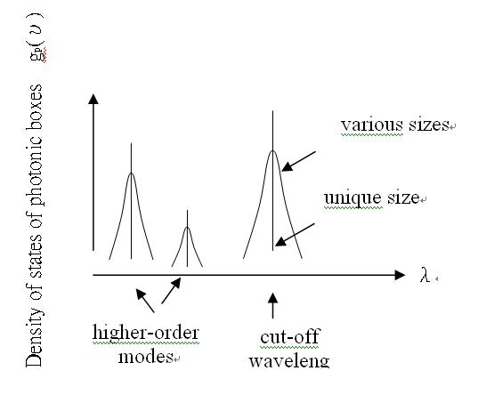
Fig. 1 Density of states of the photonic boxes. Unique box size will exhibit a delta function,
and various sizes of boxes will broaden the density of states.
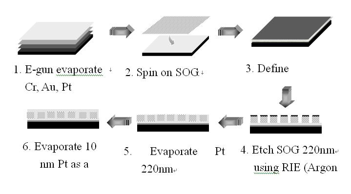
Fig. 2 Fabrication steps of the photonic boxes.
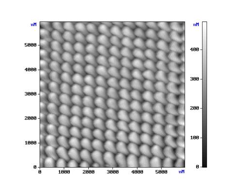
Fig. 3 AFM image of the fabricated photonic boxes.
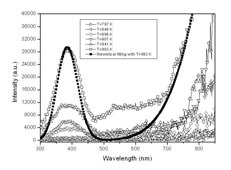
Fig. 4 Measured spectra of radiation from heated photonic boxes at different temperatures and theoretical fitting with formula (1) at T=983K.
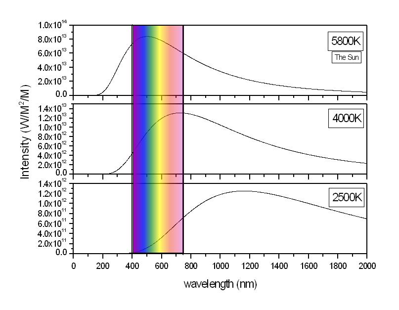
Fig. 5 Traditional tungsten bulb has only about 5% energy conversion coefficient with visible light range under 2500K.
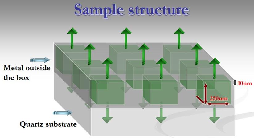
Fig. 6 Box size dominates the peak wavelength.
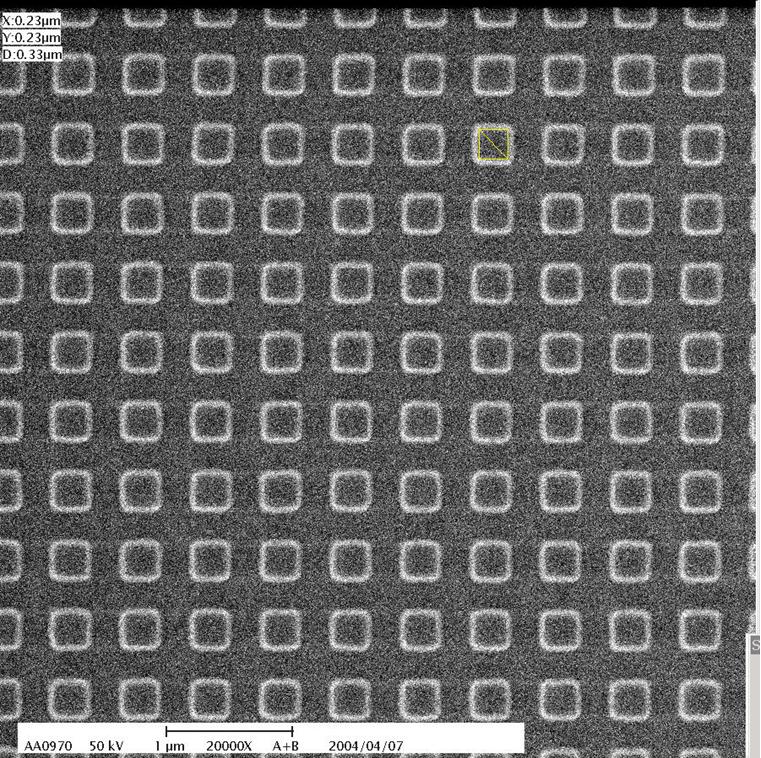
Fig. 7 SEM image of the photoresist to fabricate metallic photonic boxes
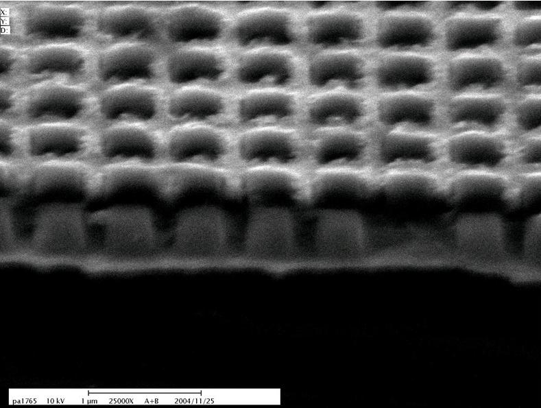
Fig. 8 SEM image of the metallic photonic boxes
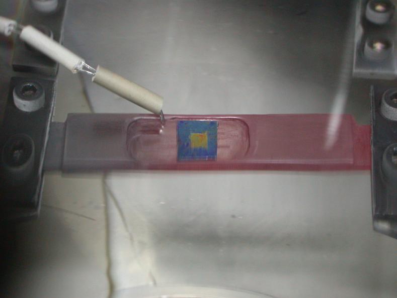
Fig. 9 Image of the metallic photonic boxes before heating
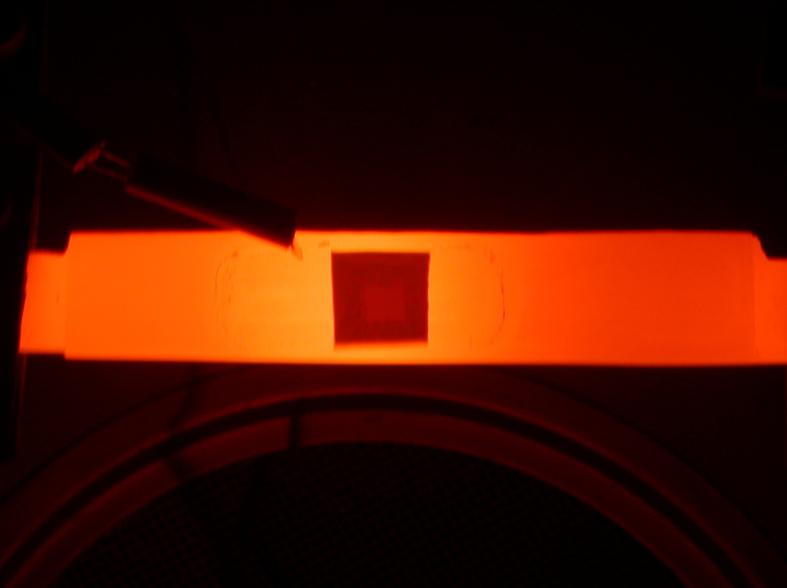
Fig. 10 Image of the metallic photonic boxes at high temperature
中文摘要:
此研究之目的為研究金屬三維共振腔結構之黑體輻射的發光特性。傳統黑體輻射的能量分佈在可見光區域僅只有5%(溫度在2200°C時),意即
有大部份能量的光浪費掉而無法作用在照明的用途。我們利用金屬三維共振腔的概念製作奈米金屬光子盒,可以將光侷限在一個金屬包附的三
維共振腔內,設計對應的尺寸,限制光發出的波長。我們的研究發現,當使用尺寸為200奈米的金屬光子盒,可以使其發出最長為400奈米的光
譜,並且能大輻降低長波長波段能量的光。當溫度僅達到1000°C時,在400奈米的光強度比長波長波段的光強度高上5倍之多。若設計不同尺寸
的金屬光子盒,在加熱到高溫後,也可以使其對應不同波長的光。此一概念大幅改變傳統黑體輻射的概念,使金屬光子盒在較低的溫度就可以
達到可見光的輻射,未來在照明產業上的應用極具潛力。
主題六:矽光子
研究人員:洪士哲、趙家忻、許書嘉、林信伯、王鼎鑫
英文摘要:
Silicon photonics has been an active research field of integrated optics, where low-cost, compact, and integrated optical components are dedicatedly pursued.
Compact, small-core waveguides, however, suffers from excessive scattering loss due to the sidewall roughness, which prohibits building dense integrated
optoelectronic circuits.
In our laboratory, KrF excimer laser reformation is presented as an alternative method for sidewall smoothing. It is capable of reducing root-mean-square (RMS)
roughness from 14 nm to 0.24 nm. This technique has no limitation on thermal budget if resistant sol-gel coatings for high power laser are employed for
selective exposure. This advantage makes the process compatible with modern VLSI electronics.
The principle of laser reformation for smooth Si waveguides is to melt the sidewall by a high energy laser pulse at an incident angle, as illustrated in Fig. 1. The
molten Si of the sidewall reforms due to the surface tension and hence gives the name of this technique. In this technique, the quantity of energy absorbed by
silicon from excimer laser highly depends on incident angle of the laser beam due to transmission coefficient of this electromagnetic wave at interface. In order
to selectively exposure sidewall rather than top surface and substrate, the incoming laser beam is designated to illuminate on the Si ridge at a greatly inclined
angle. This configuration allows laser to mainly melt the sidewall at a suitable energy density.
It is difficult to directly examine the sidewalls by atomic force microscopy (AFM) because of the limited sharpness of the scanning tips. Therefore, a
correspondence of the roughness reduction after laser reformation is made from Si planar surfaces. A silicon wafer was etched by RIE as the planar surface. The
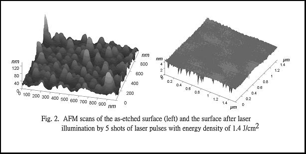
as-etched Si surface has a RMS roughness of 14 nm, as shown in Fig. 2 (left). Laser illumination with an energy density of 1.4 J/cm2 is applied at normal
incidence. By one shot of laser pulse, the RMS roughness of the laser-reformed surface reduces to 0.28 nm. By 5 shots of laser pulses, the RMS roughness
reduces to 0.24 nm. The AFM photo of Si surface illuminated by 5 shots is shown in Fig. 2 (right). As shown in Fig. 2, the highest protrusion on the as-etched
surface even exceeds 100 nm. Such a high roughness reduction is due to surface tension which enables the surface area to be the minimum by nature.
Good surface quality of Si waveguides is required in many optoelectronic devices, especially in Si light emitters. Surface quality can be quantitatively
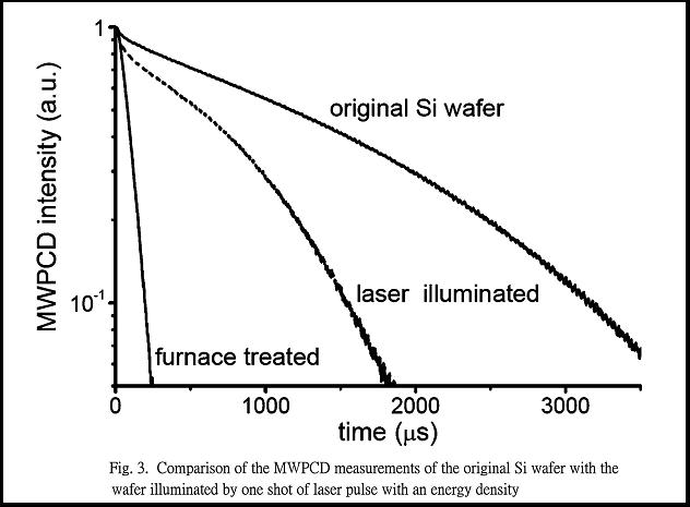
characterized by surface recombination velocity (SRV), which is proportional to the surface defects and impurities. SRV can be extracted from the carrier
lifetimes in microwave-reflection photo-conductance- decay (MWPCD). The MWPCD responses before and after laser reformation are shown in Fig. 3. The
carrier lifetime of a furnace-treated Si wafers is also depicted for comparison. The furnace-treated sample is placed in Ar at a temperature of 800o C for 10 min.
Ar is used to replacing air to prevent oxidation. The original wafers are grown by float-zone method with a thickness of 550 μm, a doping concentration of
1015 cm-3 and a resistivity of 10~50 ohm-cm. The carrier lifetime of the original wafers is 1818 μs, fitted from Fig. 3. It becomes 981 μs after illumination
with one shot of the KrF excimer laser pulse with an energy density of 1.4 J/cm2 at normal incidence. The SRV increases 26 cm/s after laser illumination. In
contrast, the carrier lifetime of the furnace-treated wafer reduces to 106 μs. The SRV increases 489 cm/s. The comparison between the increased SRVs in the
laser-reformed wafers and the furnace-treated wafers indicates that the damage by the former method is 95% less than the latter one.
In conclusion, sidewall smoothing by KrF excimer laser reformation for silicon ridge waveguide is presented. AFM measurement shows the RMS roughness is
reduced from 14 nm to 0.24 nm. Scattering loss of waveguides with such a small sidewall roughness is calculated to be 0.033 dB/cm. Compared to other
processes like hydrogen annealing, dry oxidation and wet chemical etching, the laser reformation technique shows unique capabilities of flattening protrusions
as high as 100 nm and of selective exposure. Good surface quality shown in MWPCD measurements also supports the laser-reformation method to fabricate
optoelectronic devices.
中文摘要:
積的波導由於側表面粗糙,承受著更多的散射損耗,導致難以製作高密度的光電子電路。
我們實驗室發展一種新的方法,KrF準分子雷射重整,來改善側表面的粗糙。它能將方均根粗糙由14 nm降
至0,24 nm。如果我們塗佈一層可扺抗高能量雷射的保護層於欲保護的電子元件上,將使這個方法沒有溫度
上的限制。這個優點使得這個製程相容於現在的VLSI電子產品。
雷射重整原理是利用高能量的雷射將矽波導的側表面融化,如圖1所示。側表面融化的矽由於表面張力
重新形成。在這個方法中,矽吸收雷射的能量與雷射的入射角有關。這是由於電磁波在介面穿透與反射的
基本原理。為了選擇性地照射雷射光在側表面上,而不是上表面與基板,必須將樣品傾一個很大的角度。
這樣的架設使得雷射可以主要融化側表面。
一般來說,我們很難用原子力顯微鏡來檢視側表面。這是由於掃描的針具有有限的角度。因此,我們製
作一個相對應的矽平面來檢視雷射重整後的平面粗糙。剛蝕刻後的矽表面具有14 nm的RMS粗糙,如圖2(
左)所示。經過一發垂直入射能量密度為1.4 J/cm2的雷射脈衝,表面粗糙變為0.28 nm。經過五發後,表面
粗糙降至0.24 nm。如圖2(右)所示,最高的突出可達到超過100 nm。如此優異的粗糙降低是由於表面張
力使表面面積達到最小。
好的矽波導表面品質在很多光電子元件上是需要的,尤其是矽發光元件。表面品質可以由表面復合速率
(surface recombination velocity)來觀察。表面復合速率正比於表面缺陷和雜質的數目。它可以由微波反射光導
衰減(microwave-reflection photo-conductance- decay)所測得的載子生命週期得知。圖3顯示雷射重整之前
與之後的微波反射光導衰減反應。由高溫爐處理的矽樣品也同樣用來比較。這個樣本被放置在800度C氬氣
中十分鐘。其中,氬被用來取代空氣以防止氧化。一開始的樣品是厚度550 μm由,float-zone方法長晶,摻
雜濃度為
期為1818 μs。在照射過一發垂直入射能量密度為1.4 J/cm2的雷射脈衝,它變為981 μs。表面復合速率增加
這兩者增加的表面復合速率比較,雷射處理對樣品的傷害比高溫爐處理的傷害少了95%。
整理以上所提到的,我們提供一種雷射重整的方法來平滑矽脊柱波導的側表面。原子力顯微鏡量測顯示
RMS粗糙由14 nm降低至0.24 nm。計算其散射損耗將降至0.033 dB/cm。比較其他方法,如氫退火,乾氧化,
溼蝕刻等方法,雷射重整具有選擇性和高達100 nm平坦能力的優異特性。好的表面特性也保證了雷射重整
用來製作光電元件。
主題七: 半導體雷射以及半導體光放大器
研究人員: 趙俊傑
英文摘要:
The development of semiconductor lasers and amplifiers results in revolutionary advances in the information technology, such as laser disks and fiber
communications. Because these devices are pumped directly by current injection, they are suitable to be combined with various electronic circuits in different
applications. However, like other optical gain materials, the gain-bandwidth of the semiconductor materials is limited by the intrinsic material properties, such as
bandgap. Our research is focused on increasing the gain bandwidth of active semiconductor optical devices by band-gap engineering technique. Combining
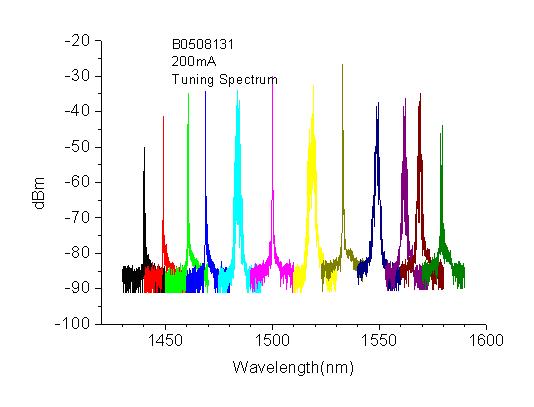
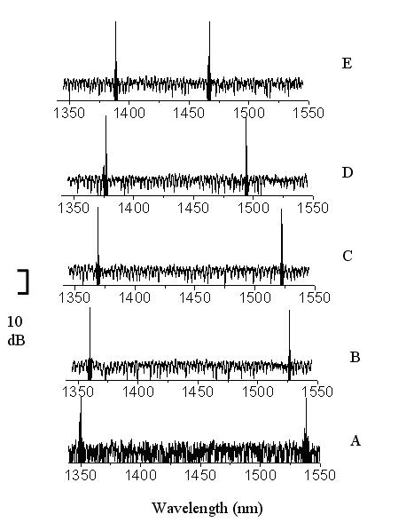
QWs with different transition wavelengths is one example. We have successfully applied this technique on InP based devices and wavelength tunable lasers with
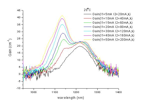
240nm tuning range (1300nm~ 1540nm) is demonstrated. Combining QDs with different sizes is another example. The gain bandwidth of the QD SOAs
fabricated in our lab also achieves more than 200nm(1050nm~1250nm).
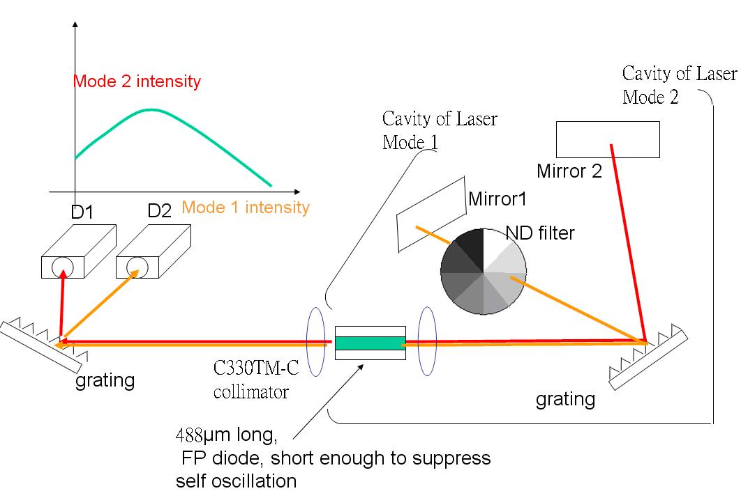
Because carriers in these broad band optical devices are distributed among states with large energy separation, the carrier dynamics of these devices are different
from conventional QW and QD devices. When two laser modes share the gain provided by one broad-band device and the wavelength separation of the two
laser modes is large, the increase of intensity in one lasing mode could enhance the intensity of another mode. This contrasts the usual competition effects in
which the intensity increment of one lasing mode suppressed the intensity of another mode.
中文摘要:
半導體雷射以及半導體光放大器的進步促成了雷射光碟片以及光纖通訊等資訊科技的革命性發展。因為這些元件事以電流直接激發,它們很適
合在各種應用裡與電子電路做直接的結合。然而,與其他光學增益材料相同的,半導體材料的光學增益頻寬也是被材料本身的特性所限制(如能
隙)。的我門的研究主題是以能帶工程的方式增加主動半導體光學元件的增益頻寬。在單一元件裡組合有不同發光波長的量子井即是此類方法的
一個例子。我們把這個技術應用在以InP為基礎的材料上,並成功的做出有240nm(1300nm~ 1540nm)可調頻寬的波長可調雷射。在單一元件裡組
合有不同發光波長的量子點則是能帶工程的另一個例子。用這個技術,我們實驗室所製造出來的量子點光學放大器其增益頻寬可以達到
200nm(1050nm~1250nm)以上。
在這些元件裡,載子所分布的能態其能量差異比較大,因此這些光學元件裡的載子動力學與一般的量子井及量子點元件不同。如果兩道雷射光
共用同一個寬頻元件所提供的增益而且其波長差異頗大,增加其中一道雷射光的強度會使得另一道雷射光的強度也會隨之增加。這與一般所觀
察到的載子競爭效應,增加其中一道雷射光的強度使得另一道雷射光的強度減弱,恰恰相反。
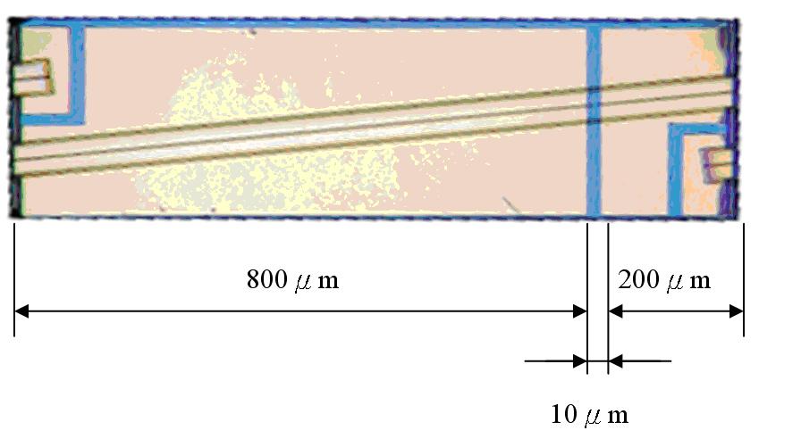
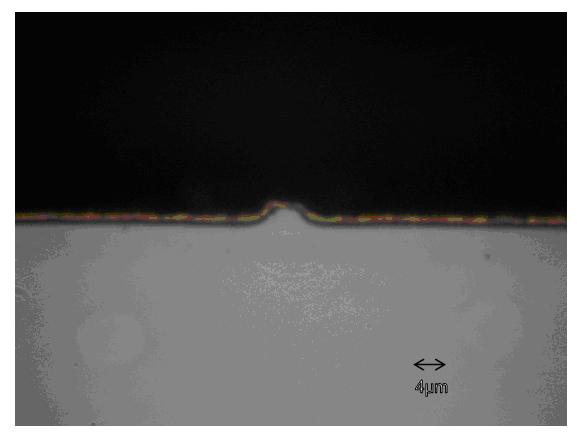
圖示:
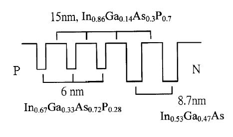
1. epi-structure of the broad band QW device,寬頻量子井元件的磊晶結構
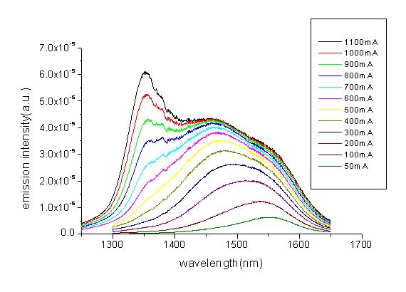
2. EL Spectrum of the broadband QW SOA,寬頻量子井光放大器的電激發光頻譜
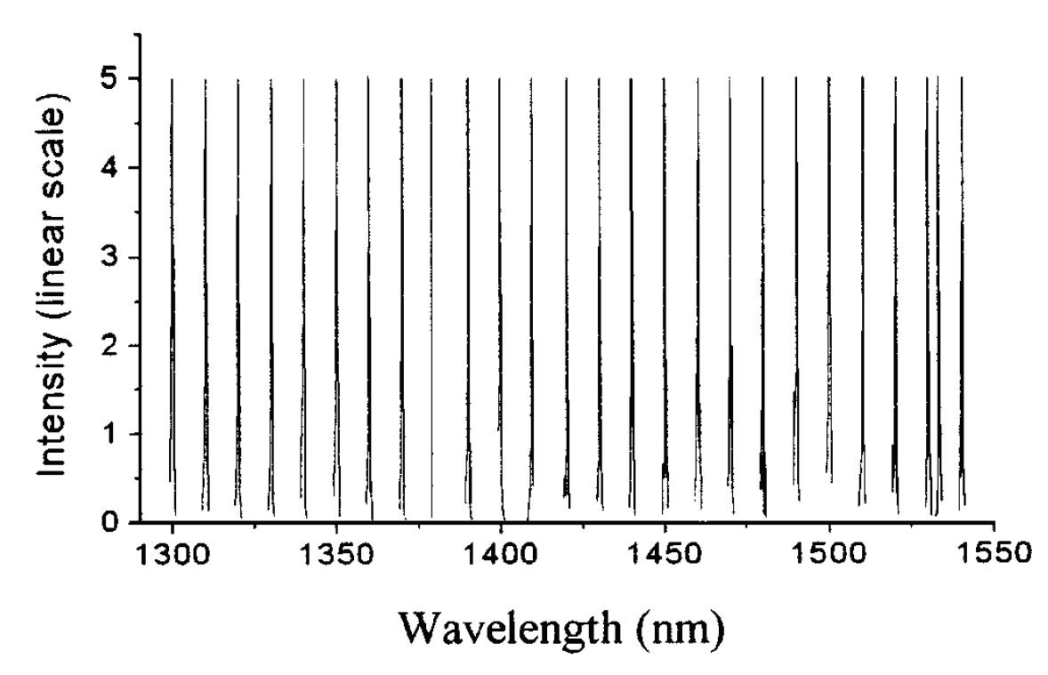
3.Emission Spectrum of the wavelength tunable laser波長可調雷射的輸出頻譜
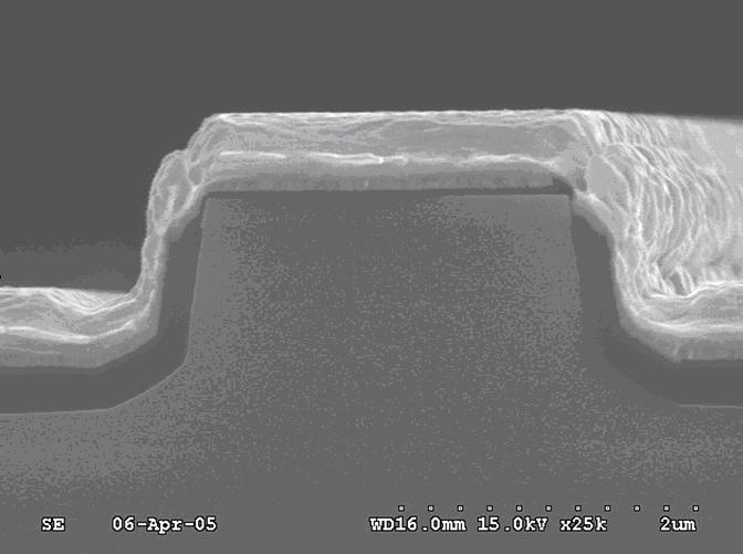
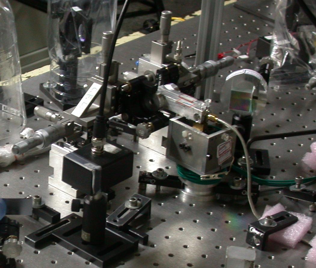
4.SEM of the facet of a SOA device,光放大器的元件的發射面照片
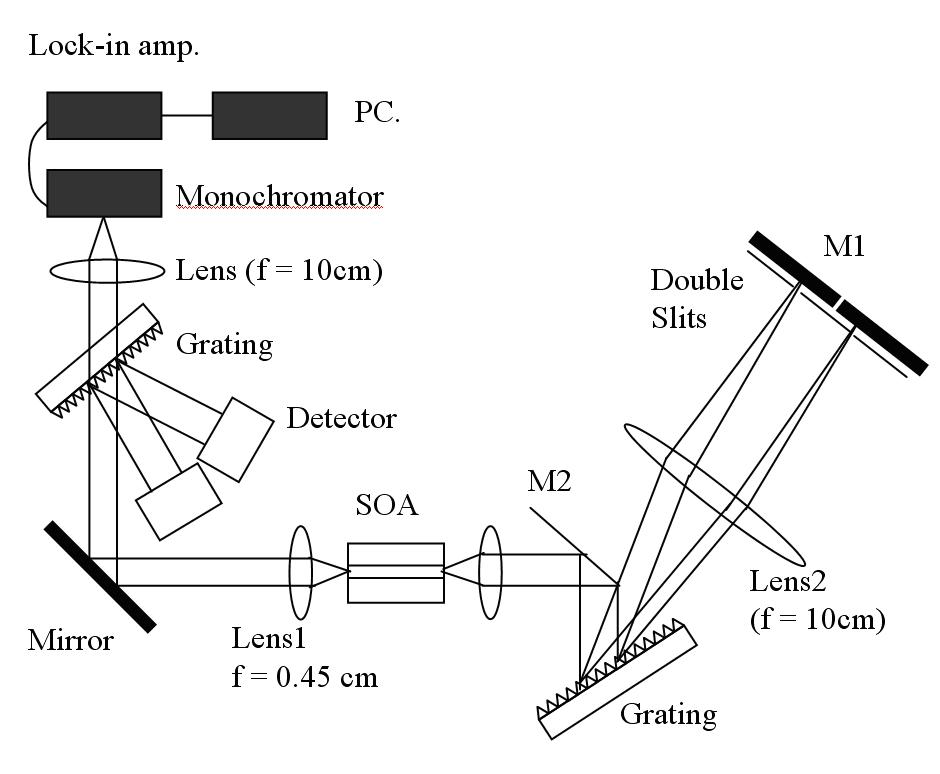
5.Cavity of the wavelength tunable laser波長可調雷射的共振槍結構
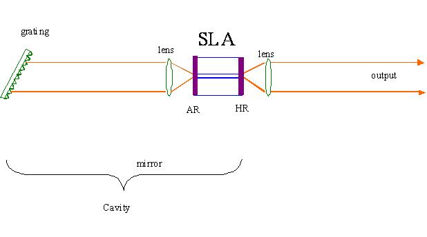
6.Experimental Setup of the Wavelength Tunable Laser波長可調雷射的實驗設置
7-1.Emission spectrum of the CW wavelength tunable laser, CW 波長可調雷射的輸出頻譜
7-2雙波長雷射的共振腔設計
7-3雙波長雷射的輸出頻譜
8. quantum dot broad band SOA, 量子點Broad Band QD SOA
9. gain spectrum of the quantum dot SOA
10-1. Facet of the QD SOA
10-2.量子點雙波長雷射的共振腔設計
主題八: 矽微米球共振腔
研究人員: 許書嘉 、 洪士哲
英文摘要:
Microspheres support ultra-low-loss whispering-gallery modes (WGMs) when evanescently excited from adjacent waveguiding structures. The high quality
factor (Q) and small mode volume associated with WGMs makes the microspheres suitable for numerous optical devices, such as microlasers, narrow optical
filters, optical switching, ultrafine sensing, displacement measurement, rotation detection, high-resolution spectroscopy, and Raman sources. However, most of
the research with spherical structures is based on noncrystalline materials such as glass or polymers. Little literature reported microspheres on crystalline
materials, like semiconductor, in the past.
Since silicon is the dominating material in current integrated circuit industry, fabricating microspheres on a Si-based substrate contributes to compact and low-
cost photonics for mass-market applications. Here, we present a technique applying the homogenized KrF excimer laser reformation to fabricate Si spheres on
the SOI platform. It is capable of fabricating Si spheres with extremely smooth surface. AFM measurement shows that the root-mean-square roughness (RMS-
roughness) of the surface of the fabricated sphere is smaller than 0.1 nm. In addition, the selective exposure of excimer laser makes the high power laser only
work on the desired region. This outstanding property makes the process compatible with modern ULSI electronics. Furthermore, single-crystalline was
amazingly observed after total transformation of the Si profile from a rod into a sphere. In this paper, we describe the laser reformation technique and the
fabrication process in detail. The fabricated results are examined by scanning electron microscopy (SEM), atomic force microscopy (AFM) and tunneling
electron microscopy (TEM).
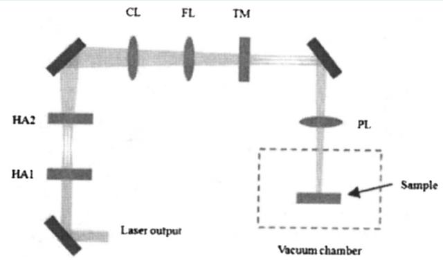
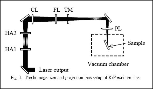
Fig.1 The diagram of homogenized KrF excimer laser reformation system.
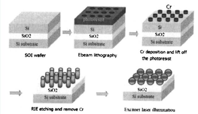
Fig.2 The flow chart of fabrication process.
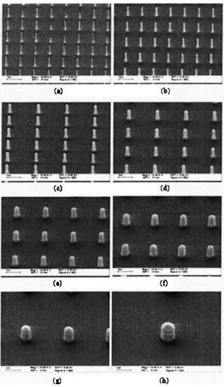
Figs.3 The 30 degree-tilted SEM images of the samples after RIE etching.
The diameters of the Si rods are (a) 40 nm, (b) 85 nm, (c) 170nm, (d) 210 nm, (e) 320 nm,
(f) 450 nm, (g) 660 nm, and (h) 940 nm.
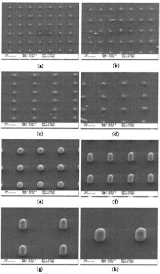
Figs.4 The SEM images of Si structures after excimer laser reformation.
Figs. 4 (a)-(h) are corresponding structures to Figs. 3.
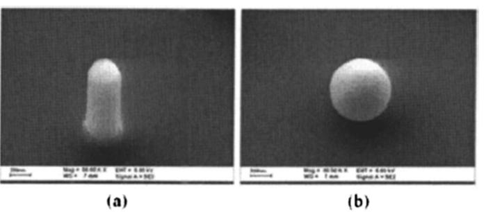
Figs.5 50000x, 30 degree tilted SEM images in the spherical case. (a) Before illumination (b) After illumination.
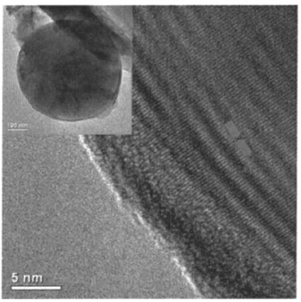
Fig.6 TEM image of the fabricated Si sphere. The insert figure is the TEM profile of the detected sphere.
中文摘要:
微米球能夠達到超低光損耗的迴廊共振模態,其擁有超高的品質因子(Q-factor)以及很小的模態體積,這使得微米球可以被應用於很多的光學元
件,其中包括了微米雷射(microlasers)、窄頻寬光濾波器(narrow optical filters)、光子開關(optical switching)、超細微靈敏感測器(ultrafine sensing)、
位移偵測(displacement measurement)、rotation detection、高解析頻譜(high-resolution spectroscopy)和拉曼源(Raman sources)。然而,大多數研究製作
微米球結構都採用非晶材料,例如玻璃或高分子材料,只有很少數的文獻報導使用晶體材料製作微米球,例如半導體材料。
因為矽材料是目前積體電路主要的材料,製作矽微米球於矽基板上將可以整合於低成本的矽基電路當中。這裡,我們展示了利用準分子雷射退
火重新塑造矽微米結構成矽微米球。原子利顯微鏡的測量發現微米球的表面粗糙度低至0.1奈米,此外。準分子雷射擁有選擇照射特定區域的功
能,可以只照射在所需得區域,這個優點未來將可以整合於積體電路的製程當中。更進一步地,我們發現矽微米球有很好的結晶特性,利用穿
透式電子顯微鏡發現其結構為單晶結構。
最新消息 研究領域摘要 指導教授 研究計畫 報帳資訊 實驗室成員 相關連結 回首頁